Calculating Fabry-Pérot transmission via Net Radiation Method or the Generalized Transfer-Matrix- Method
Updated:
One of the key components to understand how the hyperspectral camera behaves is to know the transmission profile of the scanning Fabry-Pérot interferometer (SFPI). The mirrors of the SFPI consist of a 5 mm thick ZnSe substrate onto which an anti-reflective coating is deposited on one side, while a dielectric mirror is coated on the other side. The materials and thicknesses are presented in the following table
| AR material | Thickness [nm] | Mirror material | Thickness [nm] | |
|---|---|---|---|---|
| ThF4 | $4350$ | Ge | $1255$ | |
| ZnSe | $250$ | ZnS | $20$ | |
| ThF4 | $940$ | ThF4 | $1785$ | |
| ZnSe | $500$ | ZnS | $20$ | |
| ThF4 | $340$ | Ge | $510$ | |
| Total thickness | $\mathbf{6380}$ | $\mathbf{3590}$ |
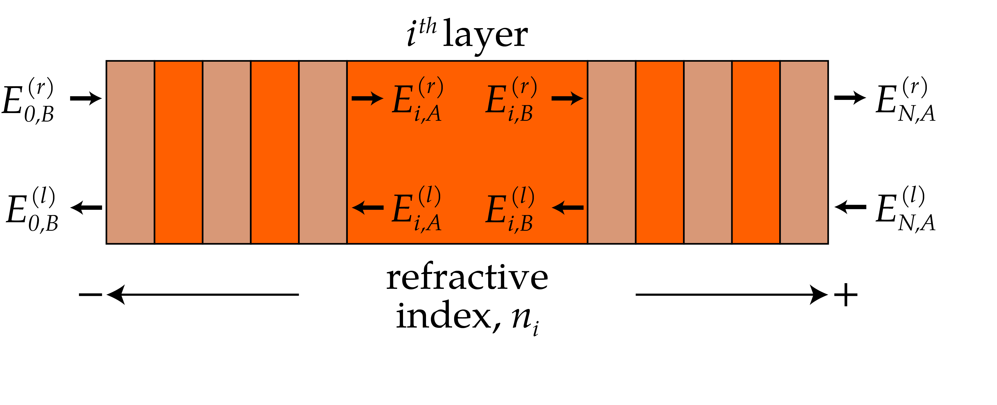
In order to calculate the transmission through the SFPI, we must know how the electric field evolves as the light travels through the thin film stack. As the light passes through the interface between two materials, a part of it is reflected and a part is transmitted. Also, as the light propagates through space, it is going to gain a phase, which is very important in thin film stacks as constructive and destructive interference is the underlying mechanism, which make the thin-film coatings work. Therefore the following notation will be used to describe the electric field at certain key points in the stack (Fig. 1). $E_{i,B}^{(r)}$ describes the complex field of the electric field of a rightwards moving wave at the immediate left side of the boundary between the $i^\textrm{th}$ and $(i+1)^\textrm{th}$ layer in the thin-film stack. Similarly, $E_{i,B}^{(l)}$ represents the field of the leftward moving wave at the same location. The field on the immediate right side of that same interface are denoted $E_{i+1,A}^{(r)}$ and $E_{i+1,A}^{(l)}$ for the rightward and leftward moving waves respectively.
Net-radiation method (NRM)
What happens to the electric field as it traverses the material boundary is described by the complex Fresnel reflection and transmission coefficients. For the time being, we will only consider light of normal incidence as this allows us to disregard the direction of polarization. Therefore, the transmission coefficient describing a wave moving form the $i^\textrm{th}$ to the $(i+1)^\textrm{th}$ layer is simply
\[\begin{align} \label{eq:fresnel_t} t_{i \rightarrow i+1} = \frac{2n_i}{n_i + n_{i+1}}, \end{align}\]where $n_i$ refers to the refractive index of the $i^\textrm{th}$ layer. Similarly, the reflection coefficient becomes
\[\begin{align} \label{eq:fresnel_r} r_{i \rightarrow i+1} = \frac{n_i - n_{i+1}}{n_i + n_{i+1}} \end{align}\]Finally, we just need the phase gained by a wave traveling a distance, $d$, through the $i^\textrm{th}$ layer of the stack:
\[\begin{align} \label{eq:phase} p_i = \exp\{-j2\pi n_i d / \lambda\}, \end{align}\]with $j$ being the imaginary unit: $j^2 = -1$
This means that we can relate the electric fields using
\[\begin{align} \label{eq:e_fileds} E_{i,B}^{(r)} &= p_i E_{i,A}^{(r)} \\ E_{i,B}^{(l)} &= r_{i \rightarrow i+1} E_{i,B}^{(r)} + t_{i + 1 \rightarrow i} E_{i+1,A}^{(l)} \\ E_{i,A}^{(r)} &= r_{i \rightarrow i-1} E_{i,A}^{(l)} + t_{i -1 \rightarrow i} E_{i-1,B}^{(l)} \\ E_{i,A}^{(l)} &= p_i E_{i,B}^{(l)} \end{align}\]This can be rearranged to a system of linear equations (by moving everything to the right-hand side of the equations) and can be solved using conventional methods. In a simple example of having a single thin-film with semi-infinite materials on either side, the matrix would be:
\[\begin{align} \label{eq:M_reg} \begin{bmatrix} -1 & 0 & 0 & 0 & 0 & 0 & 0 & 0 \\ r_{0 \rightarrow 1} & -1 & 0 & t_{1 \rightarrow 0} & 0 & 0 & 0 & 0 \\ t_{0 \rightarrow 1} & 0 & -1 & r_{1 \rightarrow 0} & 0 & 0 & 0 & 0 \\ 0 & 0 & 0 & -1 & 0 & p_1 & 0 & 0 \\ 0 & 0 & p_1 & 0 & -1 & 0 & 0 & 0 \\ 0 & 0 & 0 & 0 & r_{1 \rightarrow 2} & -1 & 0 & t_{2 \rightarrow 1} \\ 0 & 0 & 0 & 0 & t_{1 \rightarrow 2} & 0 & -1 & r_{2 \rightarrow 1} \\ 0 & 0 & 0 & 0 & 0 & 0 & 0 & -1 \\ \end{bmatrix} \begin{bmatrix} E_{0,B}^{(r)} \\ E_{0,B}^{(l)} \\ E_{1,A}^{(r)} \\ E_{1,A}^{(l)} \\ E_{1,B}^{(r)} \\ E_{1,B}^{(l)} \\ E_{2,A}^{(r)} \\ E_{2,A}^{(l)} \\ \end{bmatrix} = \begin{bmatrix} -E_0 \\ 0 \\ 0 \\ 0 \\ 0 \\ 0 \\ 0 \\ 0 \\ \end{bmatrix} \end{align}\]Where the initial electric field incident on the stack is $E_{0,B}^{(r)} = E_0$ and the leftward going wave after the thin-film is $E_{N,A}^{(l)} = 0$. This can be extended to an arbitrary number of layers. In the following code snippet it is demonstrated how the matrix, A, is constructed. The refractive indices of all the layers are stored in n.
1
2
3
4
5
6
7
8
9
10
11
12
13
14
15
16
17
18
19
20
21
22
23
24
25
26
27
def reflection_coef(n1, n2):
    return (n1-n2)/(n1+n2)

def transmission_coef(n1, n2):
    return 2*n1/(n1+n2)

def phase(n, d, lam):
    return np.exp(-1j*2*np.pi*n*d/lam)

for lam in lams:
	# refractive matrix of each layer
        n = np.array([1, refrac_Ge(lam), 1], dtype = np.complex_)
        ###################################
        ####### Constructing matrix #######
        ###################################
        A = -np.eye((len(n)-1)*4, dtype = np.complex_)
        for i in np.arange(1, int(A.shape[0]/4)):
            A[(i*4-3), (i*4-3)-1] = reflection_coef(n[i-1], n[i])
            A[(i*4-3), (i*4-3)+2] = transmission_coef(n[i], n[i-1])
            A[(i*4-2), (i*4-2)-2] = transmission_coef(n[i-1], n[i])
            A[(i*4-2), (i*4-2)+1] = reflection_coef(n[i], n[i-1])
            A[(i*4-1), (i*4-1)+2] = phase(n[i], d[i], lam)
            A[(i*4), (i*4)-2] = phase(n[i], d[i], lam)
        A[-3, -4] = reflection_coef(n[i], n[i+1])
        A[-3, -1] = transmission_coef(n[i+1], n[i])
        A[-2, -4] = transmission_coef(n[i], n[i+1])
        A[-2, -1] = reflection_coef(n[i+1], n[i])
In this way it is possible to calculate the electric fields at all interfaces at once. Finally, the reflectance and transmittance can be calculated by
\[\begin{align} \label{eq:transmittance} T = \frac{n_N}{n_0} \left|t_{0 \rightarrow N} \right|^2 = \frac{n_N}{n_0} & \left|\frac{E_{N,A}^{(r)}}{E_{0,B}^{(r)}} \right|^2 \\[1.25em] \end{align}\] \[\begin{align} \label{eq:reflectance} R = \left|r_{0 \rightarrow N} \right|^2 = &\left|\frac{E_{0,B}^{(l)}}{E_{0,B}^{(r)}} \right|^2 \end{align}\]Transfer Matrix Method (TMM)
In the case of the SFPI, we are mostly interested in its transmittance and reflectance of the entire stack, and therefore do not necessarily need to know the electric fields at every interface. Another method commonly used to describe light propagating in a thin-film stack is known as the Transfer Matrix Method (TMM). It is possible to ‘collapse’ the entire thin-film stack into a single $2\times 2$ system transfer matrix ($\mathbf{\mathcal{S}}$) relating the right- and left-going electric fields on the left side of the stack to the fields on the right side of the stack. This transfer matrix takes into account all the interfaces and accumulated phase throughout the stack and reduces it into a single matrix operation. We are therefore going to convert equation (\ref{eq:fresnel_t}), (\ref{eq:fresnel_r}), and (\ref{eq:phase}) into matrices which relate the electric fields on either side of an interface and in either end of the same layer.
When the light traverses an interface, some light will be reflected and some will be transmitted. This can be expressed as:
\[\begin{align} \label{eq:refraction_matrix} \begin{bmatrix} E_{i,B}^{(r)} \\ E_{i,B}^{(l)} \end{bmatrix} = \frac{1}{t_{i \rightarrow i+1}} \begin{bmatrix} 1 & -r_{i + 1 \rightarrow i} \\ r_{i \rightarrow i+1} & t_{i \rightarrow i + 1} t_{i + 1 \rightarrow i} - r_{i \rightarrow i+1}r_{i + 1 \rightarrow i} \end{bmatrix} \begin{bmatrix} E_{i+1,A}^{(r)} \\ E_{i+1,A}^{(l)} \end{bmatrix} = \mathbf{\mathcal{D}_{i \rightarrow i+1}} \begin{bmatrix} E_{i+1,A}^{(r)} \\ E_{i+1,A}^{(l)} \end{bmatrix} \end{align}\]Here, $\mathbf{\mathcal{D}_{i \rightarrow i+1}}$ is referred to as the refraction matrix. A similar matrix can be constructed describing the phase the light accumulates by propagating through the layer.
\[\begin{align} \label{eq:phase_matrix} \begin{bmatrix} E_{i,B}^{(r)} \\ E_{i,B}^{(l)} \end{bmatrix} = \begin{bmatrix} \exp\{j2\pi n_i d / \lambda\} & 0 \\ 0 & \exp\{-j2\pi n_i d / \lambda\} \end{bmatrix} \begin{bmatrix} E_{i+1,A}^{(r)} \\ E_{i+1,A}^{(l)} \end{bmatrix} = \mathbf{\mathcal{P}_{i}} \begin{bmatrix} E_{i+1,A}^{(r)} \\ E_{i+1,A}^{(l)} \end{bmatrix} \end{align}\]In this case $\mathbf{\mathcal{P}_{i}}$ is denoted as the phase matrix. This way, the system transfer matrix can be calculated by doing successive matrix multiplication as described in:
\[\begin{align} \label{eq:system_matrix} \begin{bmatrix} E_{0,B}^{(r)} \\ E_{0,B}^{(l)} \end{bmatrix} = \mathbf{\mathcal{D}_{0 \rightarrow 1}} \left(\prod_{i = 1}^{N-1} \mathbf{\mathcal{P}_{i}}\mathbf{\mathcal{D}_{i \rightarrow i+1}} \right) \begin{bmatrix} E_{N,A}^{(r)} \\ E_{N,A}^{(l)} \end{bmatrix} = \mathbf{\mathcal{S}}_{0\rightarrow N} \begin{bmatrix} E_{N,A}^{(r)} \\ E_{N,A}^{(l)} \end{bmatrix} \end{align}\]The resulting coefficient of transmission for the entire stack can then be calculated from the system transfer matrix by
\[\begin{align} \label{eq:tmm_transmittance} \begin{bmatrix} E_{0,B}^{(r)} \\ E_{0,B}^{(l)} \end{bmatrix} & = \mathbf{\mathcal{S}}_{0\rightarrow N} \begin{bmatrix} E_{N,A}^{(r)} \\ 0 \end{bmatrix} \\[1.3em] \Rightarrow E_{0,B}^{(r)} &= \mathbf{\mathcal{S}}_{0\rightarrow N}^{(1,1)} E_{N,A}^{(r)} \\[1.3em] \Rightarrow t_{0 \rightarrow N} &= \frac{E_{N,A}^{(r)}}{E_{0,B}^{(r)}} = \frac{1}{\mathbf{\mathcal{S}}_{0\rightarrow N}^{(1,1)}} \end{align}\]The superscript $(1,1)$ refer to the element in the first row and column of $\mathcal{S}_{0\rightarrow N}$. From this it also follows that
\[\begin{align} \label{eq:tmm_reflectance} \Rightarrow E_{0,B}^{(l)} &= \mathbf{\mathcal{S}}_{0\rightarrow N}^{(2,1)} E_{N,A}^{(r)} \\[1.3em] \Rightarrow r_{0 \rightarrow N} &= \frac{E_{0,B}^{(l)}}{E_{0,B}^{(r)}} = \frac{\mathbf{\mathcal{S}}_{0\rightarrow N}^{(2,1)}}{\mathbf{\mathcal{S}}_{0\rightarrow N}^{(1,1)}} \end{align}\]The transmittance and reflectance can then be calculated in similar fashion as presented in Eq. (\ref{eq:transmittance}) and (\ref{eq:reflectance}) respectively.
A new system transfer matrix must be calculated for each individual wavelength and in the case of the SFPI also for the different mirror separations. Depending on the spectral resolution of the calculations (both in terms of wavelength and mirror separations), a large number of transfer matrices have to be calculated and can therefore be quite computationally expensive.
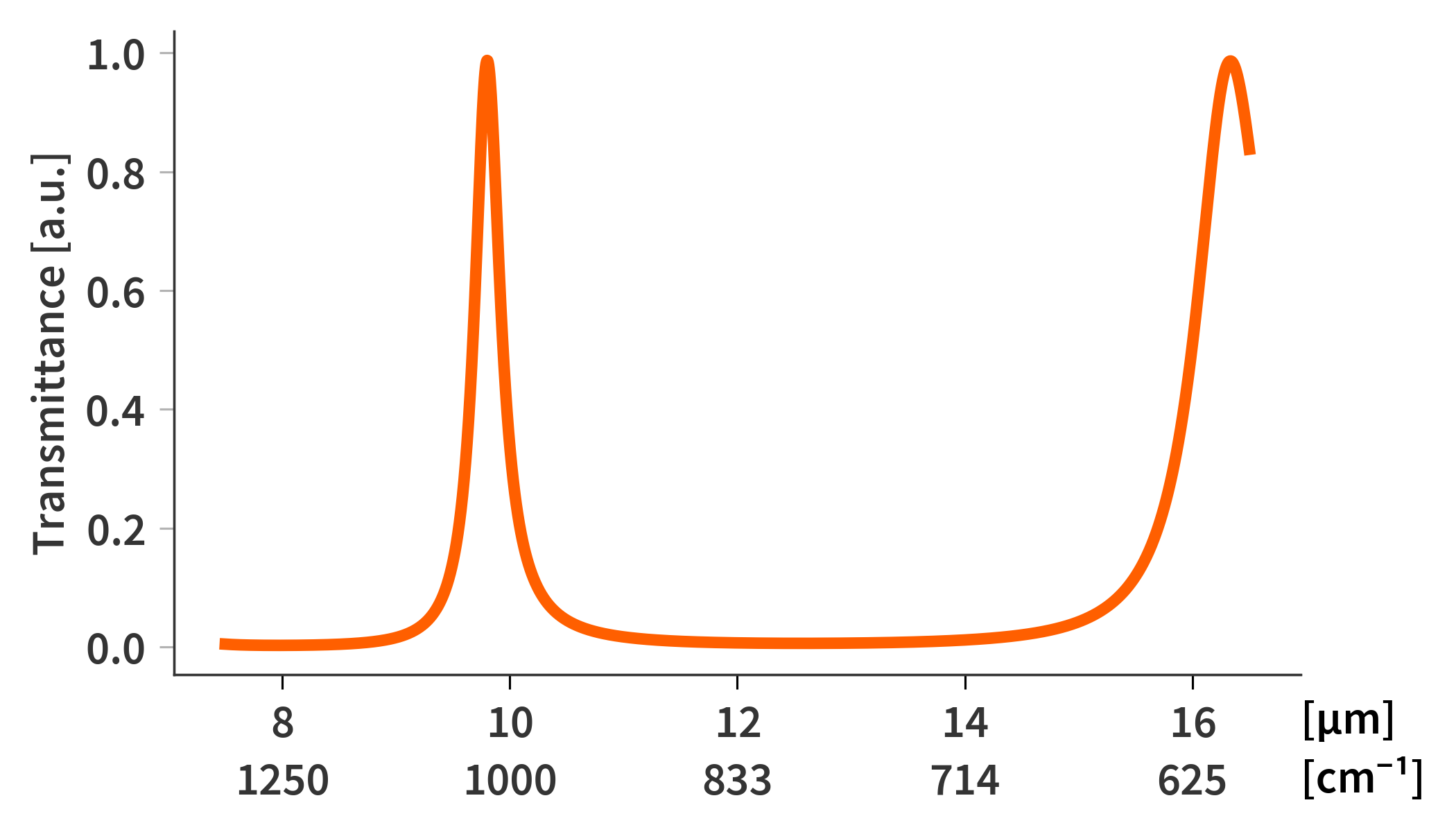
Fig. 2. illustrates the transmittance of the SFPI at a mirror-to-mirror distance of 10 µm calculated using TMM. The same result can also be achieved using the NRM. In this case only the mirror coatings are simulated as the comparatively thick substrates poses some issues for these methods as will be elaborated in coming sections. The stack therefore only contains of: semi-infinite ZnSe substrate, mirror coating, air gap, mirror coating, semi-infinite ZnSe substrate.
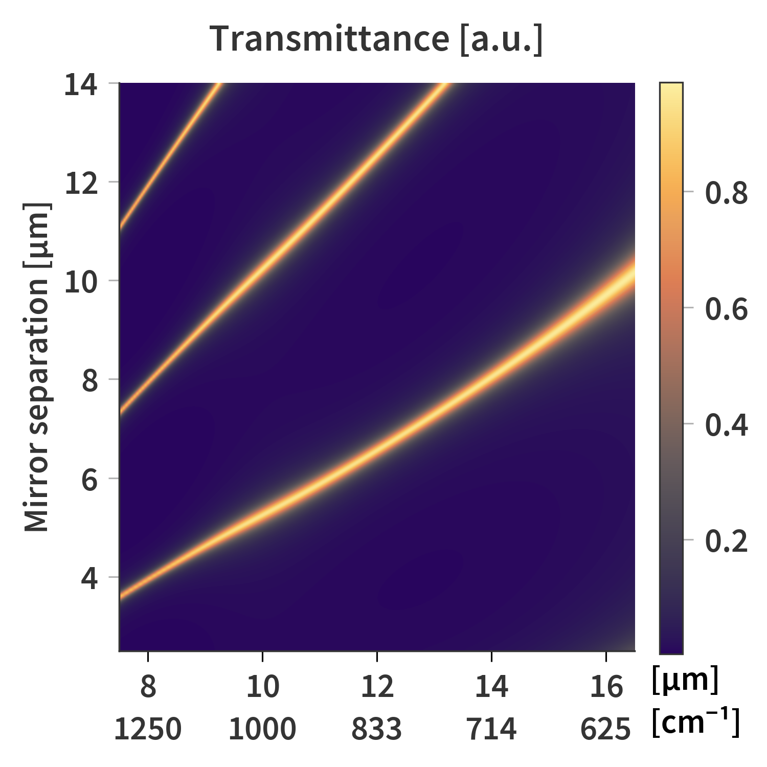
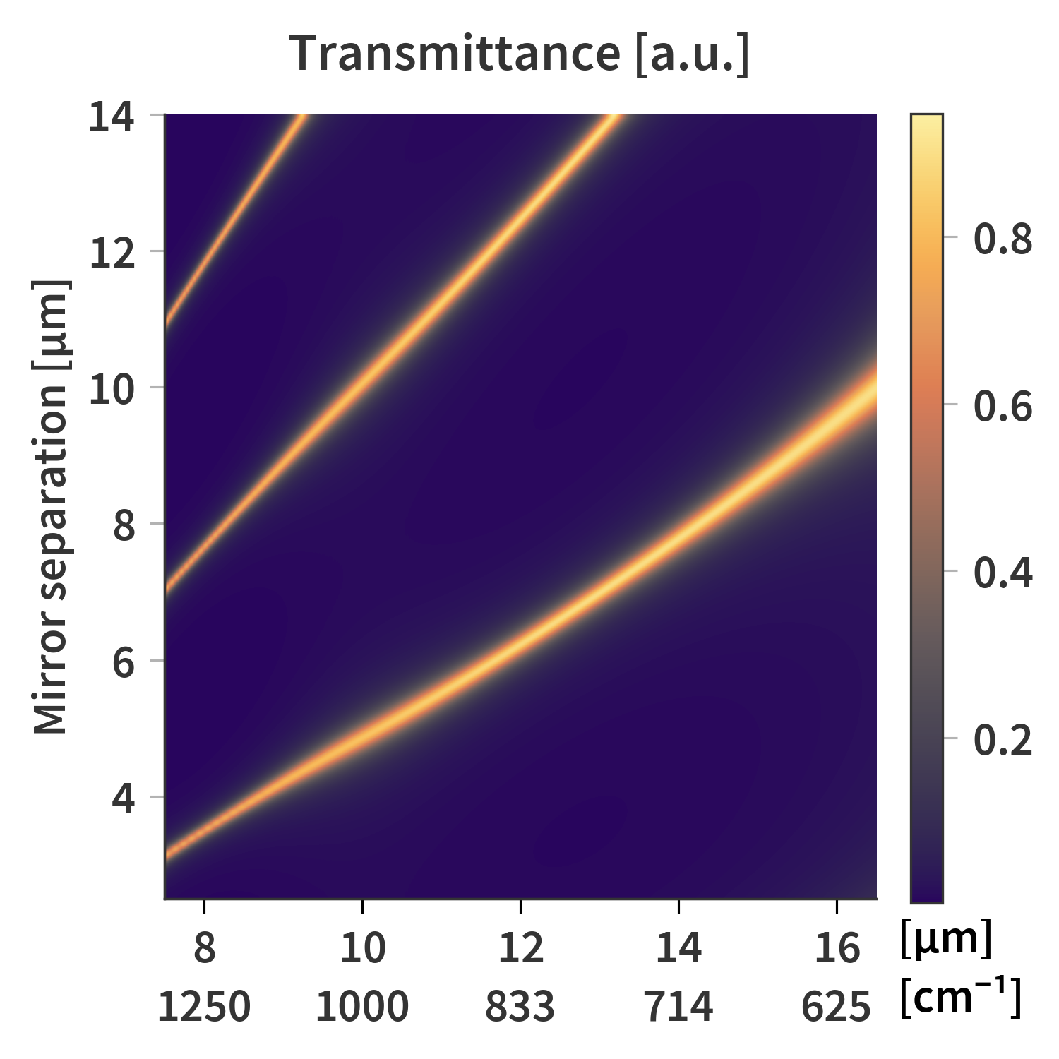
This calculation can be done for several different mirror-to-mirror distances resulting in a transmittance matrix as presented in Fig. 3.
The problem with thick substrates
Until now, the ZnSe substrates have been treated as being semi-infinite. But if the effect of the AR-coating must be included so must the substrates. The problem with the substrates is that they are way thicker (5 mm) than the coherence length of the light. Naively, the coherence length of a light source with spectral distribution, $g(k)$, can be calculated using (LibreTexts Physics):
\[\begin{align} \label{eq:coherence} \gamma(\tau) = \int_0^{\infty} g(\tilde{\nu}) e^{-2\pi j c \tilde{\nu} \tau} d\tilde{\nu} \end{align}\]Here, $\tilde{\nu} = \lambda^{-1}$ denotes the wavenumber and $c$ is the speed of light. $\tau$ is sometimes referred to as the retardation time and can be related to a distance by defining $\tau = \Delta z/c$, where $\Delta z$ is the retardation length - a.i. the length light travels in the time $\tau$. In this case we assume that the light source is a perfect black body radiator as described by the Planck distribution
\begin{align} \label{eq:BB_exitance_nu} M_{BB} (\tilde{\nu}, T) = 2\pi hc^2\tilde{\nu}^3 \frac{1}{\exp{\frac{hc\tilde{\nu}}{k_B T}} - 1} \end{align}
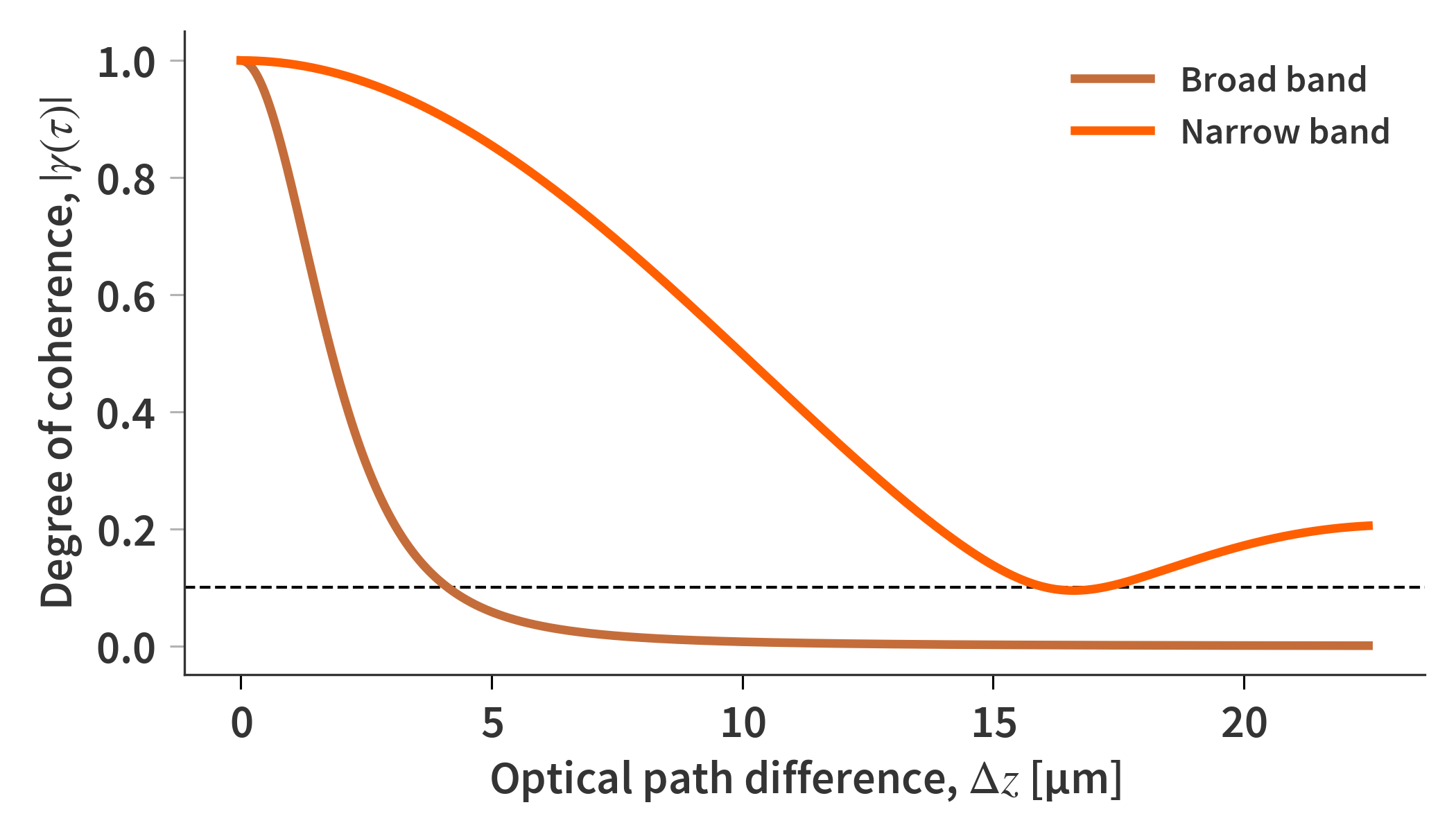
By setting $g(\tilde{\nu}) = M_{BB}(\tilde{\nu}, T)$ it is possible to calculate the degree of coherence, $|\gamma ( \tau )|$ based on Eq. (\ref{eq:coherence}) (done numerically). Fig. 4. illustrates the degree of coherence evaluated for a broad band ($\tilde{\nu} \in [0, \infty]\textrm{ cm}^{-1}$) and for a narrow band ($\tilde{\nu} \in [625, 1250] \textrm{ cm}^{-1}$). The narrow band simulates the spectral range of the sensor. If the coherence length is defined as the point at which the coherence has dropped to 10% of its starting point, the coherence lengths are found to be 4 µm and 16 µm for the broad and narrow band evaluations respectively.
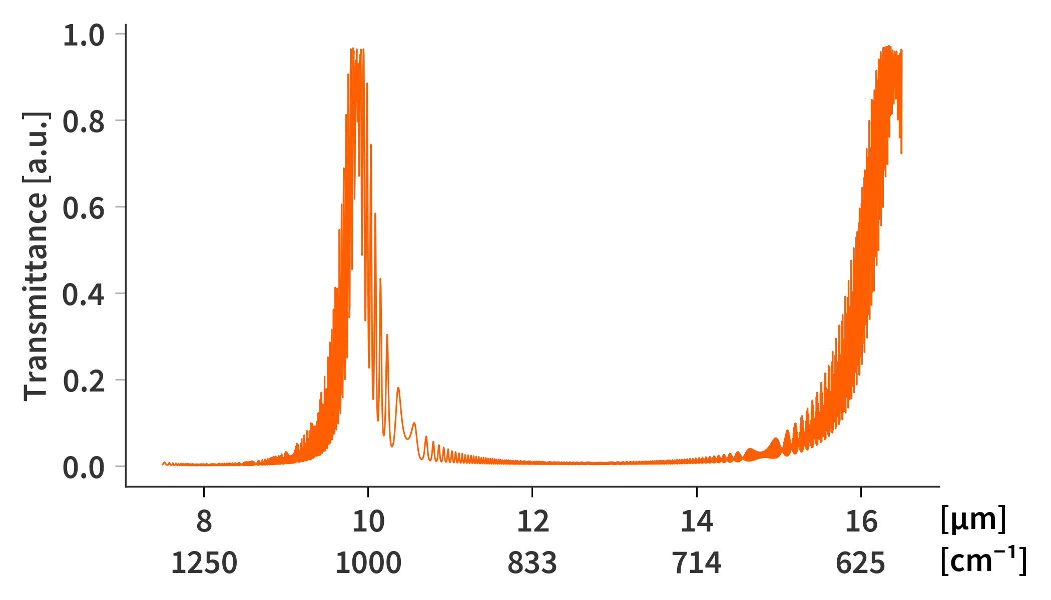
The substrates are therefore several orders of magnitudes thicker than the coherence of the light - even for the narrower band in which the sensor is responsive. Fig. 5 illustrates the issue which arises from this. Here the same SFPI is simulated as previously, but now both the thick substrates as well as the AR-coatings are included. Treating the substrate as a coherent layer as the rest of the stack results in a lot of high frequency oscillations. This is also evident in the transmittance matrix (Fig. 6) which now looks rather fuzzy.

We need a way to treat the ZnSe substrates as incoherent layers even though TMM is inherently a coherent method. In incoherent light, there is no phase information to speak of. To simulate this, one could introduce a phase offset to the ZnSe layers and ‘sample’ across many different offsets. Now, the phase matrix associated with each layer would now take another argument: the phase offset, $\delta$.
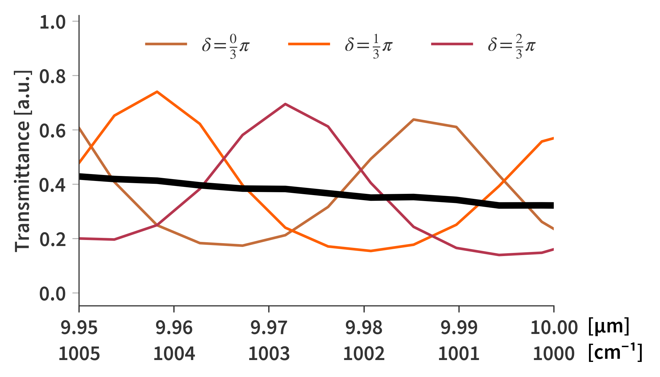
\[\begin{align} \label{eq:phase_matrix_offset} \begin{bmatrix} E_{i,B}^{(r)} \\ E_{i,B}^{(l)} \end{bmatrix} = \begin{bmatrix} \exp\{j2\pi n_i d / \lambda + \delta\} & 0 \\ 0 & \exp\{-j2\pi n_i d / \lambda + \delta\} \end{bmatrix} \begin{bmatrix} E_{i+1,A}^{(r)} \\ E_{i+1,A}^{(l)} \end{bmatrix} = \mathbf{\mathcal{P}_{i}}(\delta) \begin{bmatrix} E_{i+1,A}^{(r)} \\ E_{i+1,A}^{(l)} \end{bmatrix} \end{align}\]In practice, $\delta = 0$ for all coherent layers, while in the case of the ZnSe substrates, $\delta$ would be varied between $0$ and $\pi$. Each calculation still treats every layer as being coherent, but in the limit where $\delta$ is sampled infinitely many times, the results averages out as if the affected layers were incoherent. Luckily, It does not require an infinite amount of calculations to arrive at a satisfactory result. Fig. 7 show how three different offsets changes the resulting transmittance with their average shown as a black solid line.
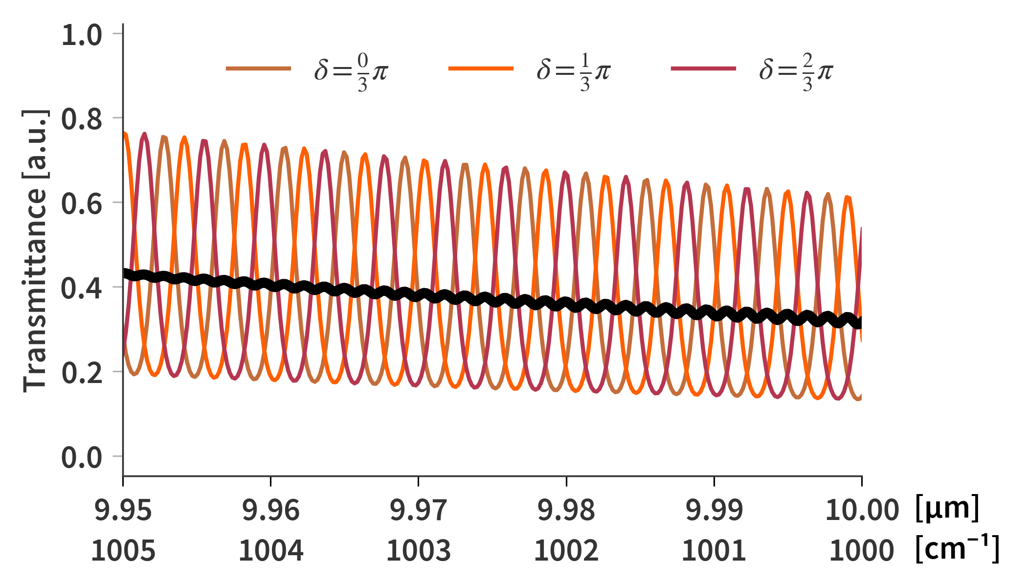
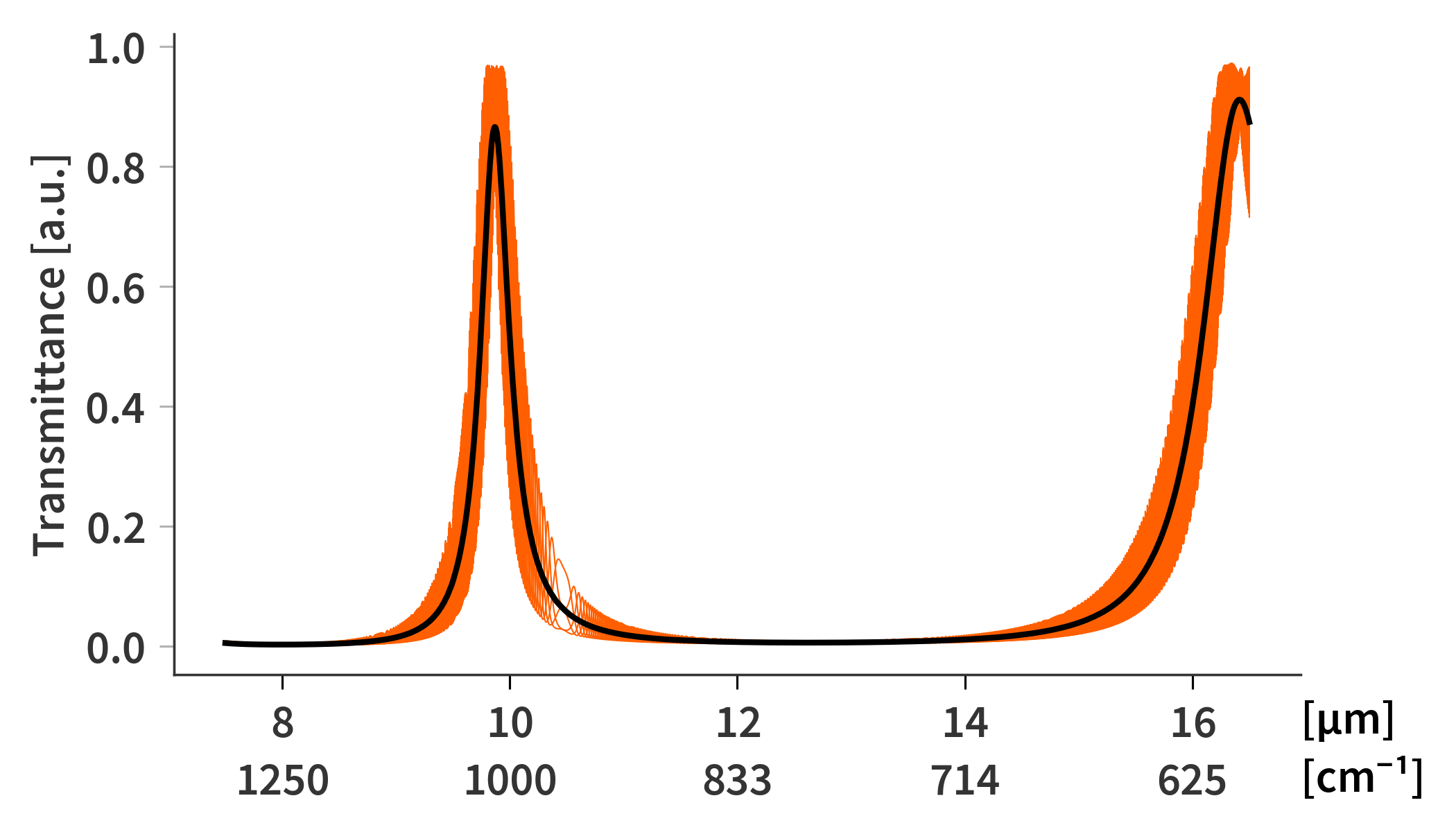
The average transmittance in Fig. 7 still exhibit some smaller oscillations, but already at 5 equidistantly sampled phases, the average transmittance spectrum has close to no fringes left caused by the ZnSe substrates as illustrated in Fig. 8 and 9 - Defiantly usable.
This method of discreetly sampling different phase offsets also opens op for the possibility of partially coherent layers as described by Santbergen et. al. Each calculation could be associated with a weight which is then used when averaging the results. A completely incoherent layers would have the weights uniformly distributed across all phases, while the partially incoherent layers would have weights decreasing with phase offset.
A note on resolution of the wavelength axis
The sampling rate of the wavelength axis must be very high in order to see all fringes shown in Fig. 7. The spectral resolution of Fig. 5 is much lower and the fringes are much broader as a result. However, due to the equidistant sampling and averaging, it is not necessary to sample with a resolution high enough to capture every single fringe. If the transmittance is sampled as coarsely as in Fig. 5 (2000 samples from $\lambda = 7.5$ µm to $\lambda = 16.5$ µm compared to 50000 samples across the same range), then the interference fringes are as shown in Fig. 10. Note that the average line is still very close to that of the high resolution calculations (Fig. 7).
Generalized Matrix Method (GMM)
While the previous method does appear to be working for incoherent substrates it still has a major drawback as it requires multiple iterations due to the phase offsets introduced by the incoherent ZnSe substrates. This becomes increasingly expensive as this is a calculation which is performed quite often. It would therefore be nice, if it is possible to take a lesser “brute force” approach. Luckily, (Katsidis et. al) have developed an approach which modifies TMM to include the incoherent layers directly in the matrix formulation.
GMM closely resembles TMM: We still try to reduce the thin-film stack to a single $2 \times 2$ transfer matrix, and the refraction and phase matrices are the same as previously. In fact - if all layers are coherent, then GMM is exactly the same as TMM. GMM makes it possible to easily include both partially coherent as well as completely incoherent layers. The partial coherence is an effect, which is caused by macroscopic surface/interface roughness. This can be modeled as a modification to the Fresnel coefficients of the refraction matrix.
\[\begin{align} \label{eq:fresnel_coefs} r_{i \rightarrow i+1} &= r_{i \rightarrow i+1}^{(0)} \exp\left[-2(sn_i \tilde{\nu})^2 \right] = \alpha r_{i \rightarrow i+1}^{(0)} \\[1.3em] r_{i+1 \rightarrow i} &= r_{i+1 \rightarrow i}^{(0)} \exp\left[-2(sn_{i+1} \tilde{\nu})^2 \right] = \beta r_{i+1 \rightarrow i}^{(0)} \\[1.3em] t_{i \rightarrow i+1} &= t_{i \rightarrow i+1}^{(0)} \exp\left[-\frac{1}{2}(s \tilde{\nu})^2(n_{i+1} - n_i)^2 \right] = \gamma t_{i \rightarrow i+1}^{(0)} \\[1.3em] t_{i+1 \rightarrow i} &= t_{i+1 \rightarrow i}^{(0)} \exp\left[-\frac{1}{2}(s \tilde{\nu})^2(n_i - n_{i+1})^2 \right] = \gamma t_{i+1 \rightarrow i}^{(0)} \\[1.3em] s &= 2\pi Z \end{align}\]Here, the $(0)$ superscripts indicate the unaltered Fresnel coefficients (for a smooth interface), and $Z$ is the RMS height of the irregularities at an interface.
Completely incoherent layers
The introduction of completely incoherent layers add some additional steps to the matrix calculations. Say the stack contains two incoherent layers (as is the case for the SFPI), then the stack must be split into smaller blocks, each of which having its own system transfer matrix. Fig. 11 illustrates how this would be done.

Fig 11: Schematic representation of SFPI stack with incoherent layers (number of layers not exact nor to scale).
The transfer matrices for each of the coherent (or partially coherent) blocks in the same way as before. Say the incoherent layers are at position $k$ and $l$. Then three blocks must be formed enclosing the two incoherent layers. The system transfer matrices are calculated as previously but separately for each block. Once these are calculated we are ready to “throw away” the phase information as we transition to and from the incoherent layers. This is done by squaring the amplitudes of Fresnel coefficients contained in the transfer matrices which will now be denoted as “intensity matrices”:
\[\begin{align} \label{eq:transfer_matrix_intensity} \mathcal{S}_{0\rightarrow k}^\textrm{int} = \frac{1}{\left|t_{0 \rightarrow k}\right|^2} \begin{bmatrix} 1 & -\left|r_{k \rightarrow 0}\right|^2 \\ \left|r_{0 \rightarrow k}\right|^2 & \left|t_{0 \rightarrow k} t_{k \rightarrow 0}\right|^2 - \left|r_{0 \rightarrow k}r_{k \rightarrow 0}\right|^2 \end{bmatrix} \end{align}\]Note that each of the coefficients can be calculated form the elements of the transfer matrix (not intensity matrix) by
\[\begin{align} \label{eq:fresnel_coefs_from_matrix} r_{0 \rightarrow k} &= \frac{\mathcal{S}_{0\rightarrow k}^{(2,1)}}{\mathcal{S}_{0\rightarrow k}^{(1,1)}} \\[1.3em] r_{k \rightarrow 0} &= - \frac{\mathcal{S}_{0\rightarrow k}^{(1,2)}}{\mathcal{S}_{0\rightarrow k}^{(1,1)}} \\[1.3em] t_{0 \rightarrow k} &= \frac{1}{\mathcal{S}_{0\rightarrow k}^{(1,1)}} \\[1.3em] t_{k \rightarrow 0} &= \frac{\mathrm{Det}\left(\mathcal{S}_{0\rightarrow k}\right)}{\mathcal{S}_{0\rightarrow k}^{(1,1)}} \end{align}\]The final thin is to define the phase matrices of the incoherent layers. This is done in a similar way by squaring the entries of the original phase matrix:
\[\begin{align} \label{eq:phase_matrix_intensity} \mathbf{P}_i^\mathrm{int} = \begin{bmatrix} \left|\exp\{j2\pi n_i d_i / \lambda\}\right|^2 & 0 \\ 0 & \left|\exp\{-j2\pi n_i d_i / \lambda\}\right|^2 \end{bmatrix} \end{align}\]The total transfer matrix for the entire stack including incoherent layers can then be calculated by combining all relevant transfer matrices and squared phase matrices:
\[\begin{align} \label{eq:final_system_matrix} \mathcal{S}^\textrm{inco} = \mathcal{S}_{0\rightarrow k}^\textrm{int} \mathbf{P}_k^\mathrm{int} \mathcal{S}_{k\rightarrow l}^\textrm{int} \mathbf{P}_l^\mathrm{int} \mathcal{S}_{l\rightarrow N}^\textrm{int} \end{align}\]$\mathcal{S}\textrm{inco}$ no longer contains any information about phase, but its matrix elements can still be used to calculate the reflectance and transmittance using.
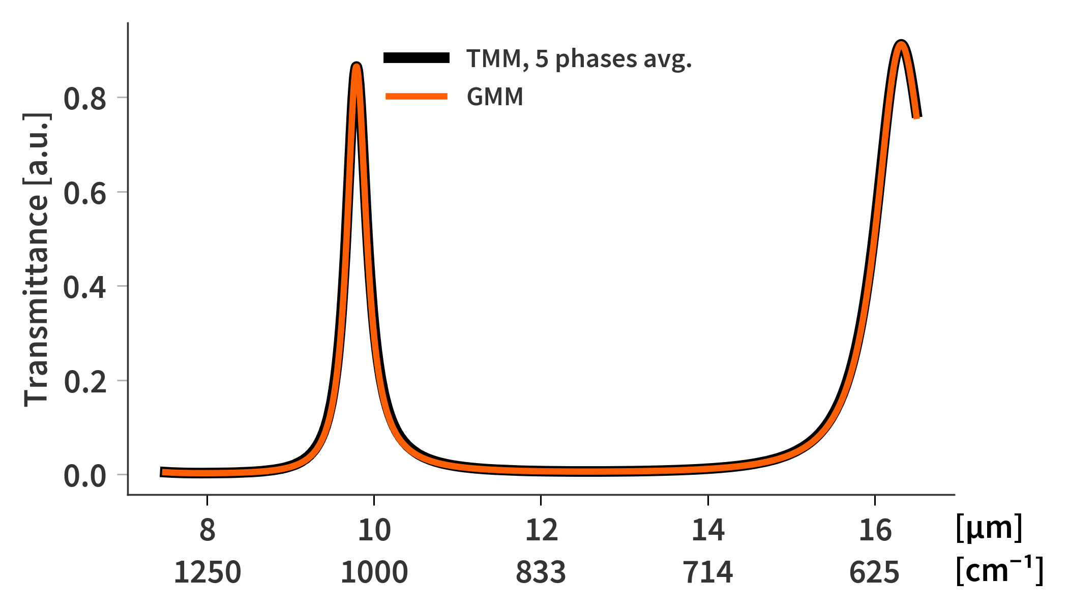
\[\begin{align} \label{eq:coherent_T_and_R} T &= \frac{n_N}{n_0} \frac{1}{\mathcal{S}^{\textrm{inco},(1,1)}} \\[1.3em] R &= \frac{\mathcal{S}^{\textrm{inco},(2,1)}}{\mathcal{S}^{\textrm{inco},(1,1)}} \end{align}\]This method yields similar results to the method described previously but without the same penalty related to performing multiple computations for simulating the phase shifts. Furthermore, there is no need to worry about the ‘phase resolution’ and averaging effects. Finally, Fig. 2 is a comparison between the transmittance found using GMM and TMM where the result of 5 different phase offsets to the ZnSe substrate layers have been averaged. Since GMM only requires one iteration, it will be the preferred way of calculating the transmittance of different mirror configurations.
